JADE Architecture with Xilinx Kintex Ultrascale FPGA offers price, power and processing performance advantages
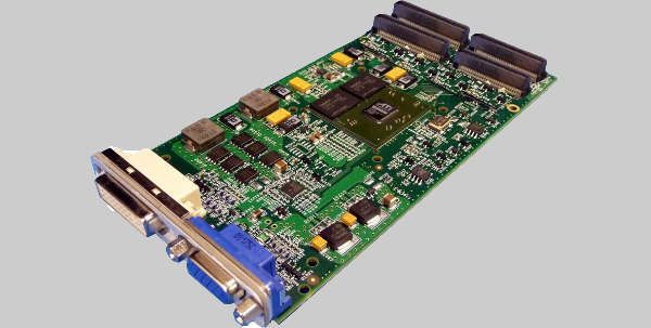
Pentek yesterday introduced the newest member of the JADE family of high-performance data converter XMC modules based on the Xilinx Kintex Ultrascale FPGA. The Model 71131 is an eight-channel, 250 MHz XMC module featuring 16-bit A/Ds with programmable multiband digital down converters (DDCs).
The Model 71131 is suitable for connection to HF or IF ports of a communications or radar system. Its built-in data capture feature offers an ideal turnkey solution as well as a platform for developing and deploying custom FPGA-processing IP. The eight channels make it especially beneficial for multi-channel phased array platforms in defense and weather radar applications where the cost per channel can be substantially reduced.
The front end accepts eight analog HF or IF inputs on front panel MMCX connectors with transformer coupling into four Texas Instruments ADS42LB69 dual 250 MHz, 16-bit A/D converters. The digital outputs are delivered into the Kintex UltraScale FPGA for signal-processing and routing to other module resources.
“Our customers are excited to take advantage of the Jade Architecture and our Navigator Design Suite,” said Bob Sgandurra, director of Product Development of Pentek. “Access to over 90 Pentek IP modules using the AXI interface has greatly eased their design effort, reducing cost and development time while eliminating worries about complex data converter interface issues.”
The Pentek JADE Architecture is based on the Xilinx Kintex UltraScale FPGA, which raises the digital signal processing (DSP) performance by over 50% with equally impressive reductions in cost, power dissipation and weight. As the central feature of the JADE Architecture, the FPGA has access to all data and control paths, enabling factory-installed functions including data multiplexing, channel selection, data packing, gating, triggering and memory control. A 5 GB bank of DDR4 SDRAM is available to the FPGA for custom applications. The Gen.3 x8 PCIe link can sustain 6.4 GB/s data transfers to system memory. Eight additional gigabit serial lanes and LVDS general purpose I/O lines are available for custom solutions.